Operational amplifier applications: Difference between revisions
rm misleading + inacc sentence |
Wtshymanski (talk | contribs) No edit summary |
||
| Line 1: | Line 1: | ||
This article illustrates some typical applications of solid-state integrated circuit [[operational amplifier]]s. A simplified schematic notation is used, and the reader is reminded that many details such as device selection and power supply connections are not shown. Those interested in construction of any of these circuits for practical use should consult a more detailed textbook such as ref. 1 below. |
|||
The resistors used in these configurations are typically in the kΩ range. <1 kΩ range resistors cause excessive current flow and possible damage to the device. >1 MΩ range resistors cause excessive [[thermal noise]] and bias currents. |
The resistors used in these configurations are typically in the kΩ range. <1 kΩ range resistors cause excessive current flow and possible damage to the device. >1 MΩ range resistors cause excessive [[thermal noise]] and bias currents. |
||
| Line 146: | Line 148: | ||
:<math>I_\mathrm{D} \simeq I_\mathrm{S} e^{V_\mathrm{D} \over V_{\gamma}} </math> |
:<math>I_\mathrm{D} \simeq I_\mathrm{S} e^{V_\mathrm{D} \over V_{\gamma}} </math> |
||
putting these two formulae together and considering that the inverse of that across the diode, the relationship is proven. |
putting these two formulae together and considering that the inverse of that across the diode, the relationship is proven. |
||
Note that this implementation does not consider temperature stability and other non-ideal effects. |
|||
===Logarithm configuration=== |
===Logarithm configuration=== |
||
| Line 210: | Line 214: | ||
[[Category:Electronic amplifiers]] |
[[Category:Electronic amplifiers]] |
||
[[Category:Integrated circuits]] |
[[Category:Integrated circuits]] |
||
==References== |
|||
- Paul Horowitz and Winfield Hill, "The Art of Electronics 2nd Ed. " Cambridge University Press, Cambridge, 1989 ISBN 0521370957 |
|||
Revision as of 16:40, 13 October 2005
This article illustrates some typical applications of solid-state integrated circuit operational amplifiers. A simplified schematic notation is used, and the reader is reminded that many details such as device selection and power supply connections are not shown. Those interested in construction of any of these circuits for practical use should consult a more detailed textbook such as ref. 1 below.
The resistors used in these configurations are typically in the kΩ range. <1 kΩ range resistors cause excessive current flow and possible damage to the device. >1 MΩ range resistors cause excessive thermal noise and bias currents.
Linear circuit applications
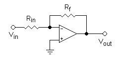
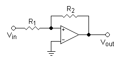
Inverting amplifier configuration
- Inverts and amplifies a voltage (multiplies by a negative constant)
- Vout = −Vin (Rf / Rin)
- Zin = Rin (because V− is a virtual ground)
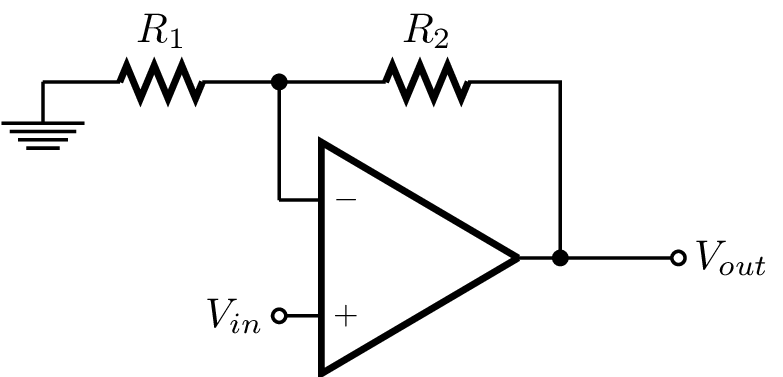
Non-inverting amplifier configuration
- Amplifies a voltage (multiplies by a constant greater than 1)
- Vout = Vin (1 + R2 / R1)
- Zin = ∞ (realistically, the input impedance of the op-amp itself, 1 MΩ to 1012 Ω)
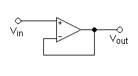
Voltage follower
- Used as a buffer, to eliminate loading effects or to interface impedances (connecting a device with a high source impedance to a device with a low input impedance)
- Vout = Vin
- Zin = ∞ (realistically, the differential input impedance of the op-amp itself, 1 MΩ to 1012 Ω)
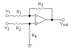
Difference amplifier
- For independent R1, R2, R3, R4 (differential amplifier):
- For R1 = R2 and R3 = R4 (amplified difference),
- For R1 = R3 and R2 = R4 (also for R1 = R2 = R3 = R4) (difference amplifier):
- Differential Zin (between the two input pins) = R1 + R2
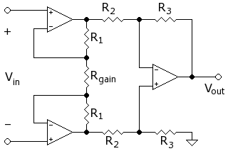
An instrumentation amplifier is made by adding a voltage follower to each input to increase the input impedance.
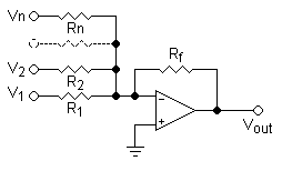
Summing amplifier
- Sums several (weighted) voltages
- Output is inverted
- For independent R1, R2, ... Rn
- V = − Rf (V1 / R1 + V2 / R2 + ... + Vn / Rn)
- For R1 = R2 = ... = Rn, and RF independent
- V = − (Rf / R1) (V1 + V2 + ... + Vn)
- For R1 = R2 = ... = Rn = Rf
- V = − (V1 + V2 + ... + Vn)
- Input impedance Zn = Rn, for each input (V− is a virtual ground)
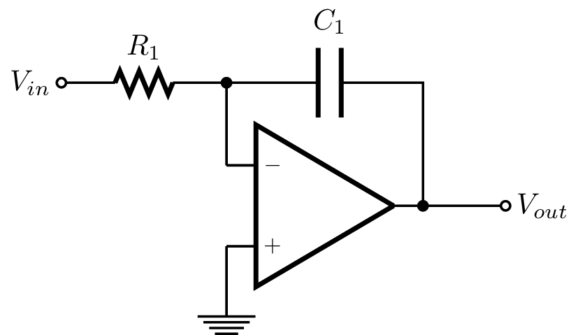
Integrator
- Integrates the (inverted) signal over time (where Vin and Vout are functions of time)
(Vinitial is the output voltage of the integrator at time t = 0.)- Note that this can also be viewed as a type of electronic filter.
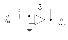
Differentiator
- Differentiates the (inverted) signal over time (where Vin and Vout are functions of time)
- Note that this can also be viewed as a type of electronic filter.
- Compares two voltages and outputs one of two states depending on which is greater
- See article for details
- Combines very high input impedance, high common-mode rejection, low DC offset, and other properties used in making very accurate, low-noise measurements
- See article for details
- A comparator with hysteresis
- See article for details
- Simulates an inductor
- See article for details
Zero level detector Voltage divider reference Zener sets reference voltage
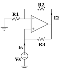
- This configuration creates a resistor having a negative value for any signal generator
- In this case, the ratio between the input voltage and the input current (thus the input resistance) is given by:
for more information see the main article Negative impedance converter.
Non-linear configurations
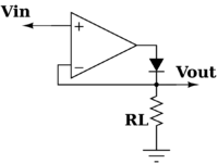
- The super diode is a configuration which behaves like an ideal diode for the load, which is now represented by a generic resistor .
- This basic configuration has some limitations. For more information and to know the configuration that is actually used see the main article super diode.
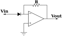
Exponential configuration
- The relationship between the input voltage and the output voltage is given by:
where is the saturation current.
- If the operational amplifier is considered ideal, the positive pin is virtually grounded, so the current through the resistor, thus through the diode, is:
where is the current through the diode. As known, the relationship between the current and the voltage for a diode is:
that, when the voltage is greater then zero, can be approximated by:
putting these two formulae together and considering that the inverse of that across the diode, the relationship is proven.
Note that this implementation does not consider temperature stability and other non-ideal effects.
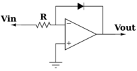
Logarithm configuration
- The relationship between the input voltage and the output voltage is given by:
where is the saturation current.
- Considering the operational amplifier ideal, then the positive pin is virtually grounded, so the current through the diode is given by:
when the voltage is greater than zero, it can be approximated by:
The output voltage is given by:
Other applications
- audio and video pre-amplifiers and buffers
- voltage comparators
- differential amplifiers
- differentiators and integrators
- filters
- precision rectifiers
- voltage and current regulators
- analogue calculators
- analogue-to-digital converters
- digital-to-analogue converters
- voltage clamps
- oscillators and waveform generators
See also
External links
- Introduction to op-amp circuit stages, second order filters, single op-amp bandpass filters, and a simple intercom
- A table of standard applications
- Hyperphysics - descriptions of common applications
- Single supply op-amp circuit collection
- Op-amp circuit collection
Additional applications
- Logarithmic amplifier
- Precision half-wave rectifier
- Precision full-wave rectifier
- Log/anti-log generators, cube generator, multiply/divide amp
- Logarithmically variable gain from a linear variable component
References
- Paul Horowitz and Winfield Hill, "The Art of Electronics 2nd Ed. " Cambridge University Press, Cambridge, 1989 ISBN 0521370957

